www.spiroprojects.com
Clock Gating Cells are indispensable components to save dynamic power. However, the backend design engineers must be prudent while placing them. In this post, I'll talk about the trade-off between timing and power that underlies the placement of clock gating cells.
Consider that your SoC has two IPs, and a single clock source. These two IPs are synchronous, and might work independently (i.e. without any interaction with the other IP) in some use-case of the chip. This entails the need of two clock gating cells. Now the question arises: where to place these clock gating cells.
- Near the sink, i.e. the clock source, or
- Near the source, i.e. the respective IPs
Let's take up pros and cons of the two placement scenarios.
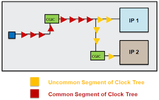
1.Clock Gating Cells placed near the source: As shown in the figure, placing the clock gating cells near the clock source, can the increase the uncommon clock path (shown in yellow).
Recall from the post: Common Path Pessimism that while doing timing analysis, the effect of OCV derates come into picture for the uncommon clock path because the clock tree buffers in the uncommon path can behave differently and hence an STA engineer needs to take into account that extra uncertainty or pessimism while doing timing analysis. Such a scenario is therefore hostile to the timing engineers. However, from power perspective this scheme is quite favorable. Since as soon as the clock gate is turned "Off", all the clock buffers in the fanout of that clock gate are also "off" or in other words, they do not toggle and hence do not dissipate dynamic power. Like any engineering problem, there exists a trade-off between two conflicting factors, and designers often need to prioritize.
2. Clock Gating Cells placed near the sink: While this scenario, with greater common path as compared to the first scenario and hence making the timing easier to met, is not friendly from the power perspective.
All the clock tree buffers in the common clock path (shown tin red) lie before the clock gate and hence would always be "on" and keep on toggling at the clock frequency, thereby dissipating dynamic power.
Solution:
The pertinence of a solution is dictated on many factors. Permissible clock latencies, power dissipation specifications, timing closure challenges and also the use-case.
Let's say we had a requirement that IP 2 will function if and only if IP 1 is on. In this case we could have placed the clock gates in series like this:
By having the two clock gates in series, we would save the dynamic power of all the clock tree buffers in the fanout of first clock gate. Moreover, the uncommon path is significantly less as compared to the scenario 1.
Again note that this solution would not work if we had the use-case where IP 1 could be "off", while IP 2 still "on".
Sign up here with your email


ConversionConversion EmoticonEmoticon